
What is Scanning Electron Microscopy?
Explore how Scanning Electron Microscopy (SEM) supports industrial applications, from failure analysis and alloy verification to cleanroom monitoring, EBSD, and EDS mapping.
Explore how Scanning Electron Microscopy (SEM) supports industrial applications, from failure analysis and alloy verification to cleanroom monitoring, EBSD, and EDS mapping.
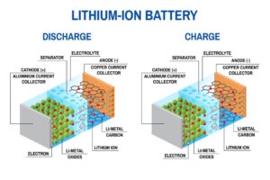
Discover how SEM and EDS techniques are transforming lithium-ion battery development. Explore structural analysis, compositional mapping, and failure detection with SciMed’s advanced SEM systems.
Discover how Energy Dispersive Spectroscopy (EDS) helps determine elemental composition in materials using electron microscopy. Applications span industry, science, and forensic research.

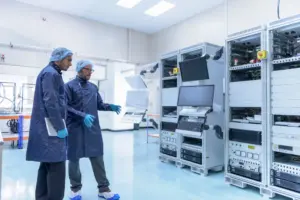
Dublin Analytical Education Electron Microscopy for Failure Mode and Effects

This guide explains how to perform AOX testing in wastewater and effluent samples in line with ISO/FDIS 9562. Learn the four key steps — sample collection, chloride/DOC removal, carbon adsorption, and AOX measurement — using the APUsim and Multi X 2500, with accuracy checks and options for AOF/PFAS analysis.
Electron paramagnetic resonance (EPR) spectroscopy can be used to study any material with unpaired electrons, known as paramagnetic materials.